- 您现在的位置:买卖IC网 > Sheet目录329 > IDT7140LA55C (IDT, Integrated Device Technology Inc)IC SRAM 8KBIT 55NS 48DIP
IDT7130SA/LA and IDT7140SA/LA
High-Speed 1K x 8 Dual-Port Static SRAM
Military, Industrial and Commercial Temperature Ranges
AC Electrical Characteristics Over the
Operating Temperature Supply Voltage Range (5)
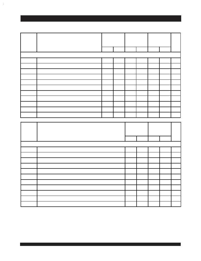
7130X20 (2)
7140X20 (2)
Com'l Only
7130X25
7140X25
Com'l, Ind
& Military
7130X35
7140X35
Com'l
& Military
Symbol
Parameter
Min.
Max.
Min.
Max.
Min.
Max.
Unit
WRITE CYCLE
t WC
t EW
t AW
t AS
t WP
t WR
t DW
Write Cycle Time (3)
Chip Enable to End-of-Write
Address Valid to End-of-Write
Address Set-up Time
Write Pulse Width (4)
Write Recovery Time
Data Valid to End-of-Write
20
15
15
0
15
0
10
____
____
____
____
____
____
____
25
20
20
0
15
0
12
____
____
____
____
____
____
____
35
30
30
0
25
0
15
____
____
____
____
____
____
____
ns
ns
ns
ns
ns
ns
ns
t HZ
Output High-Z Time
(1)
____
10
____
10
____
15
ns
Write Enable to Output in High-Z
t DH
t WZ
t OW
Data Hold Time
(1)
Output Active from End-of-Write (1)
0
____
0
____
10
____
0
____
0
____
10
____
0
____
0
____
15
____
ns
ns
ns
2689 tbl 10a
7130X55
7140X55
Com'l, Ind
& Military
7130X100
7140X100
Com'l, Ind
& Military
Symbol
Parameter
Min.
Max.
Min.
Max.
Unit
WRITE CYCLE
Write Pulse Width
Write Enable to Output in High-Z
t WC
t EW
t AW
t AS
t WP
t WR
t DW
t HZ
t DH
t WZ
Write Cycle Time (3)
Chip Enable to End-of-Write
Address Valid to End-of-Write
Address Set-up Time
(4)
Write Recovery Time
Data Valid to End-of-Write
Output High-Z Time (1)
Data Hold Time
(1)
55
40
40
0
30
0
20
____
0
____
____
____
____
____
____
____
____
25
____
25
100
90
90
0
55
0
40
____
0
____
____
____
____
____
____
____
____
40
____
40
ns
ns
ns
ns
ns
ns
ns
ns
ns
ns
t OW
Output Active from End-of-Write
(1)
0
____
0
____
ns
NOTES:
2689 tbl 10b
1. Transition is measured 0mV from Low or High-impedance voltage with Output Test Load (Figure 2). This parameter is guaranteed by device characterization but
is not production tested.
2. PLCC, TQFP and STQFP packages only.
3. For MASTER/SLAVE combination, t WC = t BAA + t WP , since R/ W = V IL must occur after t BAA.
4. If OE is LOW during a R/ W controlled write cycle, the write pulse width must be the larger of t WP or (t WZ + t DW ) to allow the I/O drivers to turn off data
to be placed on the bus for the required t DW . If OE is HIGH during a R/W controlled write cycle, this requirement does not apply and the write pulse
can be as short as the specified t WP .
5. 'X' in part numbers indicates power rating (SA or LA).
12
发布紧急采购,3分钟左右您将得到回复。
相关PDF资料
IDT7142LA55C
IC SRAM 16KBIT 55NS 48DIP
IDT7143LA25G
IC SRAM 32KBIT 25NS 68PGA
IDT7164L25YGI
IC SRAM 64KBIT 25NS 28SOJ
IDT71T75802S200PFGI
IC SRAM 18MBIT 200MHZ 100TQFP
IDT71T75902S85BGG
IC SRAM 18MBIT 85NS 119BGA
IDT71V016SA12PHGI
IC SRAM 1MBIT 12NS 44TSOP
IDT71V124SA10PHGI
IC SRAM 1MBIT 10NS 32TSOP
IDT71V256SA20PZG
IC SRAM 256KBIT 20NS 28TSOP
相关代理商/技术参数
IDT7140LA55CB
制造商:Integrated Device Technology Inc 功能描述:IC SRAM 8KBIT 55NS SB48
IDT7140LA55J
功能描述:IC SRAM 8KBIT 55NS 52PLCC RoHS:否 类别:集成电路 (IC) >> 存储器 系列:- 标准包装:2,000 系列:MoBL® 格式 - 存储器:RAM 存储器类型:SRAM - 异步 存储容量:16M(2M x 8,1M x 16) 速度:45ns 接口:并联 电源电压:2.2 V ~ 3.6 V 工作温度:-40°C ~ 85°C 封装/外壳:48-VFBGA 供应商设备封装:48-VFBGA(6x8) 包装:带卷 (TR)
IDT7140LA55J8
功能描述:IC SRAM 8KBIT 55NS 52PLCC RoHS:否 类别:集成电路 (IC) >> 存储器 系列:- 标准包装:2,000 系列:MoBL® 格式 - 存储器:RAM 存储器类型:SRAM - 异步 存储容量:16M(2M x 8,1M x 16) 速度:45ns 接口:并联 电源电压:2.2 V ~ 3.6 V 工作温度:-40°C ~ 85°C 封装/外壳:48-VFBGA 供应商设备封装:48-VFBGA(6x8) 包装:带卷 (TR)
IDT7140LA55L48B
制造商:Integrated Device Technology Inc 功能描述:IC SRAM 8KBIT 55NS 48LCC
IDT7140LA55P
功能描述:IC SRAM 8KBIT 55NS 48DIP RoHS:否 类别:集成电路 (IC) >> 存储器 系列:- 标准包装:2,000 系列:MoBL® 格式 - 存储器:RAM 存储器类型:SRAM - 异步 存储容量:16M(2M x 8,1M x 16) 速度:45ns 接口:并联 电源电压:2.2 V ~ 3.6 V 工作温度:-40°C ~ 85°C 封装/外壳:48-VFBGA 供应商设备封装:48-VFBGA(6x8) 包装:带卷 (TR)
IDT7140LA55PF
功能描述:IC SRAM 8KBIT 55NS 64TQFP RoHS:否 类别:集成电路 (IC) >> 存储器 系列:- 标准包装:2,000 系列:MoBL® 格式 - 存储器:RAM 存储器类型:SRAM - 异步 存储容量:16M(2M x 8,1M x 16) 速度:45ns 接口:并联 电源电压:2.2 V ~ 3.6 V 工作温度:-40°C ~ 85°C 封装/外壳:48-VFBGA 供应商设备封装:48-VFBGA(6x8) 包装:带卷 (TR)
IDT7140LA55PF8
功能描述:IC SRAM 8KBIT 55NS 64TQFP RoHS:否 类别:集成电路 (IC) >> 存储器 系列:- 标准包装:2,000 系列:MoBL® 格式 - 存储器:RAM 存储器类型:SRAM - 异步 存储容量:16M(2M x 8,1M x 16) 速度:45ns 接口:并联 电源电压:2.2 V ~ 3.6 V 工作温度:-40°C ~ 85°C 封装/外壳:48-VFBGA 供应商设备封装:48-VFBGA(6x8) 包装:带卷 (TR)
IDT7140SA100C
功能描述:IC SRAM 8KBIT 100NS 48DIP RoHS:否 类别:集成电路 (IC) >> 存储器 系列:- 标准包装:1,000 系列:- 格式 - 存储器:RAM 存储器类型:SRAM - 双端口,同步 存储容量:1.125M(32K x 36) 速度:5ns 接口:并联 电源电压:3.15 V ~ 3.45 V 工作温度:-40°C ~ 85°C 封装/外壳:256-LBGA 供应商设备封装:256-CABGA(17x17) 包装:带卷 (TR) 其它名称:70V3579S5BCI8
